Get involved in a new dimension!
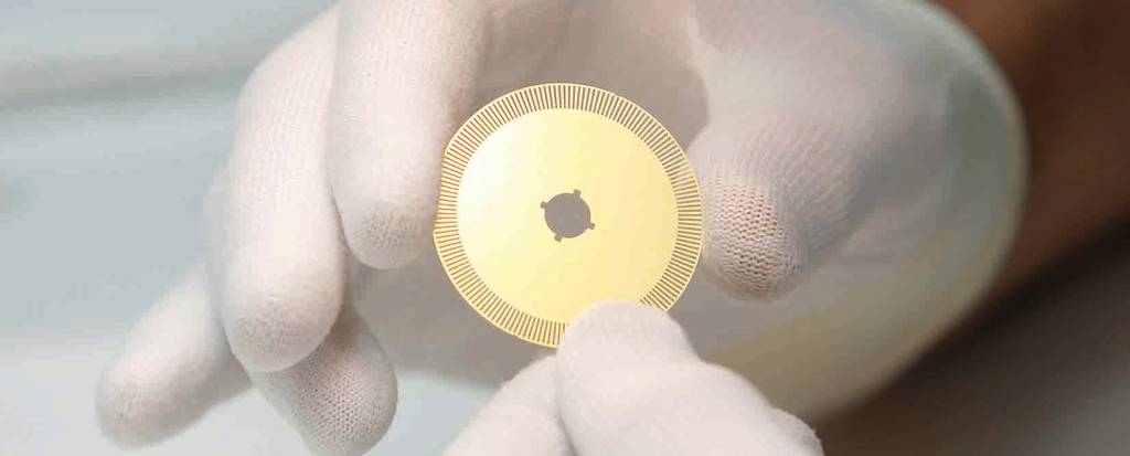
micrometal - together with its subsidiaries HP Etch and Etchform - is your one-stop shop for precision etched metal parts.
Learn more about micrometals 6 USPs that make us unique in etching technology worldwide.
Our individually tailored technologies, inline reel-to-reel etching as well as batch/ sheet etching offer you the right solution for every application.
Do you already have a precise idea? Arrange your consultation appointment here with one of our specialists right.
Overview Capability matrix chemical etching:
We have created an overview for you, which shows the performance of our photo-chemical etching process. The table also shows you the capabilities and specialities at our three different development and production sites. Find out for yourself whether our capabilities are right for you.
Please send your enquiry to [email protected].
micrometal | HP Etch | Etchform | ||
|---|---|---|---|---|
Standard materials | Stainless steel, copper and nickel and their alloys | Stainless steel, copper and nickel and their alloys | Stainless steel, copper and nickel and their alloys | |
Special materials*
* Others on request | Amorphous materials | Aluminum | Titanium, Nitinol, Molybdenum
Elgiloy, Gold, Silver | |
Production “Sheets” |
760 x 315 mm² | Max: 610 x 610 mm² | 400 x 300 mm² – Max. 600 x 600 mm² on request | |
Production “Coils” | Coil width: max. 315 mm | |||
Material thickness | 0,025 to 0,4 mm | 0,015 to 1,5 mm | 0,003 to 1,5 mm | |
Tolerance | min. +/- 0,007 mm | min. +/- 0,01 mm | min. +/- 0,01 mm | |
(guide values stainless steel) | from 0.1 mm: 10 % of the material thickness | from 0.1 mm: 12 % of the material thickness | from 0.1 mm: 12 % of the material thickness | |
Minimum web width | 0,5 x material thickness | 1 x material thickness | 1 x material thickness | |
Minimum hole/slot width | 0,8 x material thickness | 1,2 x material thickness | 1,2 x material thickness |
These are approximate values. Please contact us for more detailed information.
Etching: more than an alternative to punching or lasering.
Metal processing with the photo-chemical etching process opens up opportunities for you that are not possible using traditional processing methods. Precision, design freedom, and repeatability suddenly take on a whole new meaning. Discover for yourself in the graphic the differences and advantages that the photochemical process offers:
That's what matters:
Etching*
Punching*
Laser machining*
✓
Low change in material characteristics
✓
High cleanliness
✓
Smallest tolerances
✓
High quantities in serial production
✓
Minimum part size
✓
Good Machinability of thinnest materials (< 100 µm)
✓
Low part costs in serial production
✓
Low tooling costs
✓
High degree of design freedom and easy modification
✓
Maximum freedom from burrs
Total
* Based on a scale of 1 to 10
You can quickly see that the two most common traditional technologies punching ans laser machining do not score optimally on the selected criteria of freedom of part design, freedom from burrs, influence on material properties, cleanliness, and attainment of low tolerances. The photo-chemical etching process specifically meets these criteria and therefore should ultimately be the solution for your application.
But the photo-chemical etching process also fulfils important criteria such as low tool costs and opening up the possibility of producing large quantities of parts for series production at a very competitive and economical price.
Etching more than an alternative to classical stamping or laser processing.

High precision etching "made in Germany"
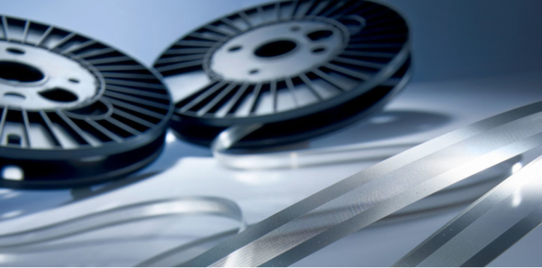
micrometal has developed a highly automated and continuous production process over decades and is thus considered the inventor of the fully cross-linked INLINE etching technology (so-called reel-to-reel etching).
High-precision glass tools, the thinnest photoresist layers and, above all, a continuous process from the raw material to the end product guarantee excellent reproducibility as well as the tightest tolerances. Regardless of the number of pieces (from a few hundred to millions) and the type of delivery (individually, in a sheet or on a reel), micrometal fulfills many customer requirements for most accurate thin metal parts.
Unique in the world — the continuous etching process
The know-how developed by micrometal means that our process differs significantly from conventional photo-chemical etching processes, laser processing, or fine blanking. Customer data is individually prepared via CAD to create a glass tool. The metal alloy requested by the customer — available as a coil — is first cleaned and then coated on both sides with photo-resist.
Already here, our process differs from the standard photo-chemical etching process. We use a patented wet paint system, which means we can create the thinnest photoresist layers, which makes our etching much more precise.
As in printing technology, the customer’s metal strip is exposed through an individually produced customised glass tool. High-precision contours are then created in the developer bath.
The metal strip then passes through an etching process that permits a wide variety of complex geometries. Cleaning and drying are followed by coordinated control steps, which can be based on spot checks as well as comprehensive automatic control and verification. Depending on customer requirements, the etched parts in the metal strip are then assembled on spools (reel-to-reel) or in individual blanks.
You benefit from this:
To meet the highest demands for accuracy, we use glass templates plotted on a laser imagesetter. Compared to photographic film templates, these glass tools have a significantly higher imaging fidelity, fine structure, and length stability. This is indispensable for the necessary double-sided, mutually referenced imaging (upper to lower glass). Compared to other tools used for metalworking (such as punches) glass masters are less expensive, with short delivery times and much longer service lives.
Thanks to the exceptional size of glass photo templates, the design area can be up to 760 mm long and 280 mm wide. The base material — often stainless steel — can be up to 330 mm wide.
While dry resist film is usually used in the photo-chemical etching industry, we achieve the thinnest photo-resist layers by using a special wet resist system. The recipe for our wet resist is a closely guarded secret! After all, it is this that enables us to create the smallest features across industry — for example hole diameter compared to the material thickness — an absolutely unique selling point.
Liquid photo-resist is more suitable for high-precision mass production in continuous processes than dry coatings (10 to 50 µm thick) because of the significantly lower coating thickness (2 to 8 µm). The result is higher reproduction accuracy.
By linking the individual process steps, the inline photo-chemical etching process enables etching in a quasi-stationary state. This enables the highest accuracies to be achieved while maintaining the tightest tolerances.
The minimum hole diameter that can be realized with our continuous etching technology is around 80% of the material thickness. At the same time, 25 µm is the thinnest standard material thickness we work with. The etching process thus makes it possible to maintain tolerances in the single-digit micrometer range.
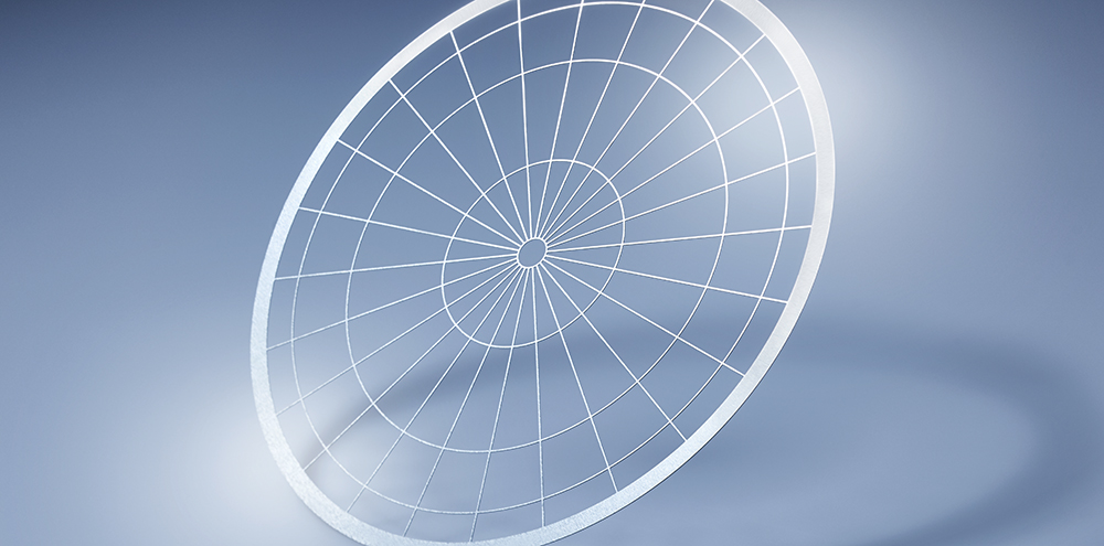
A wide variety of structures can be realized by using photo-chemical etching. Using mask technology developed in-house, we are able to control the etching process in a defined way in the third dimension. In this way, specific breakthrough geometries can be produced in three dimensions. This enables micrometal to produce complex geometries for lancets, scalpels and blades on a large scale for example.
Our process can also produce a variety of etchable hole shapes. The position of structures inserted on both sides can be very precisely matched. Etches (so-called half etches) and openings can be combined as desired. By introducing defined microfine channels, capillary effects, for example, can be used in a targeted manner.
High-precision etching technology "made in Sweden”
HP Etch Batch/ Sheet Technology is not only fast but also effective and cost-efficient. Tooling costs are very low and designs for photo-chemical masks are created digitally within a very short time frame. This allows prototypes, small, and medium quantities to be etched quickly and cost-effectively. Nickel, stainless steel, Aluminum, copper and copper alloys are among the metals processed.
› High precision with tolerances up to +/- 0.01 mm.
› Fast, small batches within one week
› Stainless steels and other steel alloys, iron-nickel alloys, copper alloys, aluminum, etc.


High-precision etching technology "made in Holland”
Etchform specializes in precision etching of virtually all metals and alloys. Among others copper, brass, phosphor bronze, beryllium, copper and many stainless steel alloys, can be processed and also special materials as titanium, nitinol, molybdenum, gold, nickel, and silver.
Etchform can also offer a wide range of processes such as electroforming or heat & surface treatment and has a strong network of partners.
Also, the company can offer production in cutting or etching from metal plates for smaller quantities or via manual processing.
