Photo-chemical etching (PCE) is now seen throughout industry as the gold standard when the demand is for geometrically complex, feature-rich, highly precise, and innovative metal parts and components.
But OEMs also need to be aware that there are different qualities of PCE available as well, and the question needs to be asked, “If you have decided to use PCE, why not contact the best photo-chemical etching company?” By the best, what we mean is the process that can attain the highest tolerances repeatably for high volumes of intricate metal parts and components.
This is where micrometal GmbH (incorporating Etchform and HP Etch) has been focusing its attention for many years, and the company has developed unique and proprietary refinements to the PCE process that out-rivals competitors in terms of control, accuracy, repeatability, speed, and cost, while at the same time producing parts with no stress-related material degradation or burrs.
Traditional PCE not only copes well with difficult geometries, it also allows design engineers enormous flexibility, facilitating the adjustment of designs right up to the point of manufacture due to the use of digital film or glass tooling. Such tooling is hugely less expensive and much faster to produce and alter than the hard steel tools, making the process ideal for prototyping (as well as low, medium, and high volume runs).
Also, as the tooling is transferred to metal through a contact printing process, there is no tool wear ensuring that the first part produced is identical to the last. PCE is also unaffected by the level of tool complexity, and it makes no difference in terms of costs or lead-time how complex the geometry of the part is and therefore the complexity of the digital film or glass tooling.
So you can see whey traditional PCE is now the go-to process for intricate metal parts and components. But what have we done to take the PCE process to the next step? Well, we have focused on a couple of the stages involved in the PCE process.
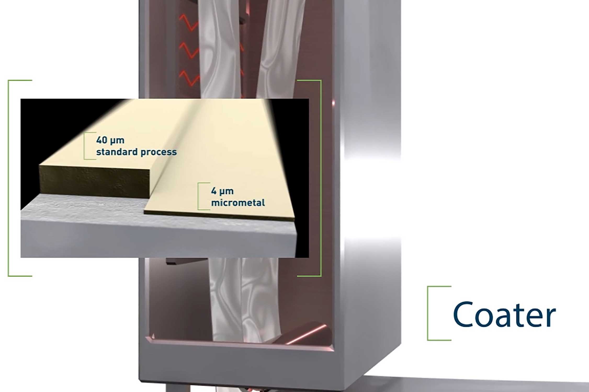
Uniquely, we use a special liquid resist system (instead of the traditional thick dry film resist) to obtain ultra-thin (2-8 micron) photoresist layers enabling a higher degree of precision in the chemical etching process. It allows us to achieve extremely small feature sizes of 25 microns, a minimum hole diameter 80% of the material thickness, and single digit micron tolerances repeatably. In addition, along with our optimised exposure system we can avoid the parallax problems typically associated with PCE.
Thick dry film resist compromises ultimate part precision and the tolerances that are attainable, and it is only able to achieve 100-micron feature sizes and a minimum hole diameter of 100-200% material thickness.
We also use photo-tooling created on glass instead of the traditional digital photo-tooling. This means we can cater for applications that require extreme precision which traditional PCE cannot achieve. Glass photo tooling can attain tolerances in the range of 1-2 microns, and negates issues with distortion due to environmental factors such as humidity that are a constant problem when using film tooling.
By way of example, over a 700 mm etch area, we can consistently achieve 5-10 micron tolerances, whereas PCE companies using film-based tooling can only claim 50-60 micro tolerances. This is why we are the go-to supplier for intricate, often safety critical, precision metal parts and components for leading names across a range of high-tech industry sectors.
You can watch our complete animated photo-chemical etching process on YouTube here.