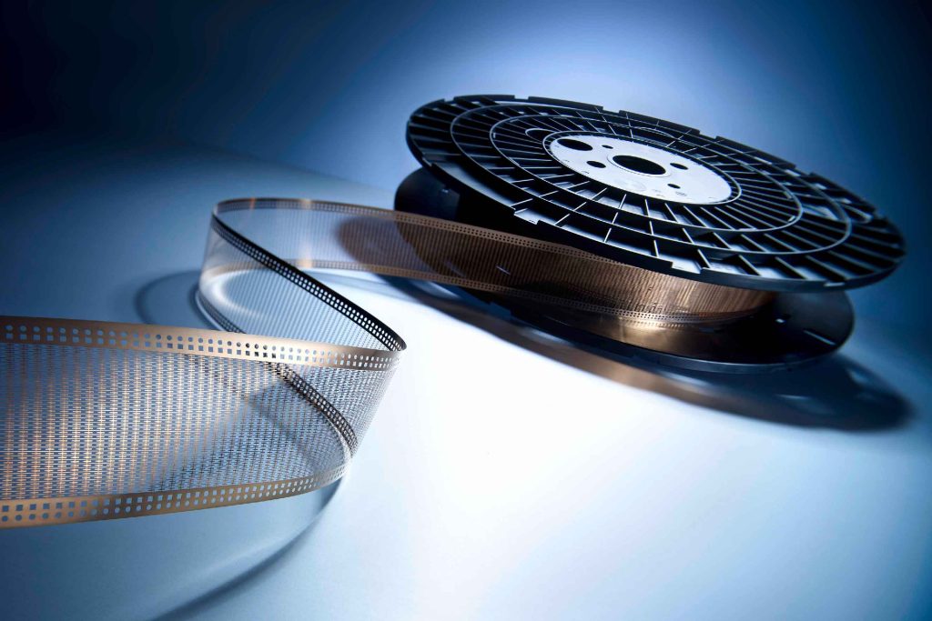
PCE making lead frames
When it comes to the cost-effective and accurate manufacture of lead frames, it is extremely important that the correct process is chosen, and supplier selection criteria are forensic to ensure optimised outcomes. The micrometal Group has developed a next-generation photo-chemical etching (PCE) process which is ideally suited to lead frame production, and gives customers the opportunity to make innovatively designed lead frames with tight tolerances repeatably and accurately while responding to the trend towards miniaturisation and weight saving.
Jochen Kern, Head of Sales & Marketing at the micrometal Etching Group says, “Lead frames are utilised in the semiconductor device assembly process, and are essentially thin layers of metal that connect the wiring from tiny electrical terminals on the semiconductor surface to the large-scale circuitry on electrical devices and circuit boards. In lead frame design, one size does not always fit all, and very often demand is for customised specifications and features, designs that enhance electrical and thermal properties, and specific cycle time requirements. micrometal has in-depth experience of lead frame manufacture using PCE for an array of different customers. We etch simple or sometimes more complex lead frames from metal and alloys that demonstrate a very low expansion rate at room temperature. These low thermal expansion alloys have found use in modern applications which require
joining of a metal to glass or ceramics and in areas that demand the same thermal expansion rates for materials to be joined in order to prevent associated problems within the joint area.”
Lead frames can often be extremely complex and also very fragile. Indeed, in many instances, geometric complexity and the requirement for extremely exacting tolerances and precision mean that PCE is not just a potentially desirable manufacturing process, but is in fact the only technology able to make certain lead frames.
When stamping lead frames, complexity adds cost, whether in low, medium, or high volume applications. The complexity of the lead frame means the necessity for a complex mould tool, and complex tooling means increased costs, increased potential for tool failure, and increased lead-times for satisfactory completion.
PCE is agnostic when it comes to the level of tool complexity, and it makes no difference in terms of costs or lead-time how complex the geometry of the part is and therefore the complexity of the digital tooling that the process uses. But PCE can also produce lead frames with tighter tolerances and finer detail than is possible with stamping, and all with minimal if any degradation and deformation of the metal being processed, and little to no likelihood of burrs or defects. Failure rates are minute, and unlike in the stamping process, every lead frame produced is absolutely flat, which is a vital prerequisite.
Kern continues, “There is no doubt that PCE is extremely well suited to the production of lead frames. However, the case for using PCE is even more compelling when the process refinements introduced by micrometal are taken into account. You see, not all PCE providers are the same. micrometal’s unique PCE process is able to achieve dimensional tolerances as a low as +/-0.005mm, small feature sizes of 25 microns, a minimum hole diameter 80% of the material thickness, and single digit micron tolerances repeatably. Compare this with traditional chemical etching which is only able to achieve a smallest feature size of 100 microns, and the smallest hole diameter is a factor of 1-2 when compared to material thickness. It is easy to see how micrometal’s PCE process opens up numerous hitherto impossible design opportunities when manufacturing lead frames.”
It is important when looking at the use of PCE for lead frame manufacture to recognise the process advantages that PCE brings to the table, but supplier selection is also important, the focus being on the expertise and experience of your chosen manufacturing partner.
Kern concludes, “Take, for example, the potential for increased margin for error due to the number of variables in the PCE process. Leading European PCE specialist micrometal has a robust, repeatable method of lead frame manufacturing due to years of experience in this area, which cannot easily be matched by other PCE service providers. To a great extent, this experience — which stretches over many decades — mitigates areas where PCE may generally be regarded to have weaknesses. The company has invested heavily in process control to reduce variation, as well as optical inspection to achieve zero parts per million failure rates. There is a huge emphasis on quality control at micrometal, and we operate under a 100% inspection process, and no failure is allowed. This is why we are proud to produce bespoke lead frames for some of the world’s leading semiconductor packaging companies.
micrometal’s tight tolerance manufacturing processes are appropriate for numerous lead frame applications, but are ideally suited to high lead/pin count, ultra-fine pitch lead frame manufacture in high volumes.